You deserve the optimal experience.
Why not add another of these best sellers to your cart?


Modern semiconductor and photonic devices require characterization techniques capable of linking physical structure, material properties and electrical performance. Spectral provides solutions for device debug, failure analysis and advanced characterization, combining sample preparation, electron microscopy, nanoprobing, AFM-based electrical measurements and microanalysis into integrated workflows.
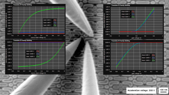
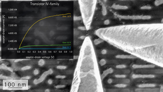
SEM-based nanoprobing enables direct electrical access to individual device structures with nanometer-scale positioning accuracy. Local I-V measurements, contact testing and electrical characterization can be performed on transistors, interconnects, contacts and other functional regions. Combined with electron-beam-based techniques such as EBIC, EBAC and current imaging, nanoprobing helps localize leakage paths, identify failure mechanisms and correlate electrical behavior with physical device structures.
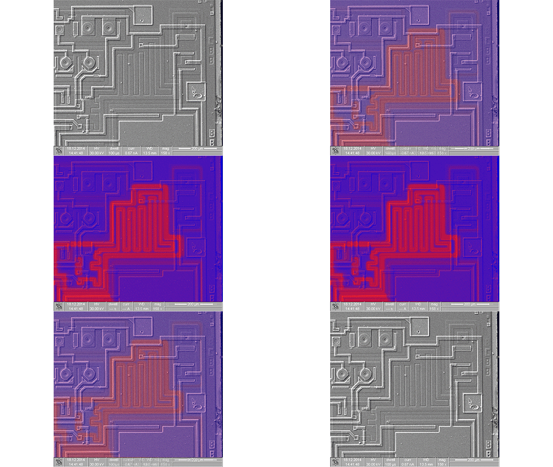
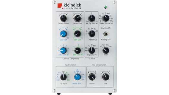
Read moreElectron Beam Induced Current (EBIC) and Electron Beam Absorbed Current (EBAC) provide powerful methods for localizing electrically active defects and investigating current flow within semiconductor devices. These techniques can reveal junction behavior, leakage paths, open circuits and buried defects that may not be visible using conventional imaging alone. By correlating electrical activity with device structure, engineers gain valuable insight into device performance and reliability.
Read moreWhile SEM reveals device structure and morphology, AFM-based techniques provide quantitative measurements of topography, conductivity, capacitance and surface potential. Integrating AFM directly inside the SEM enables structural and electrical information to be acquired from the same region of interest. This approach is particularly valuable for semiconductor devices, thin films, interfaces and advanced materials where nanoscale electrical behavior influences overall device performance.
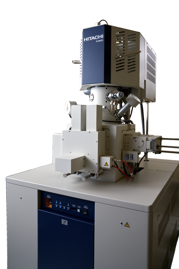
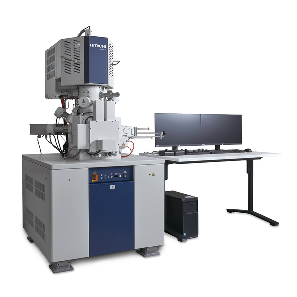
More about the Litescope AFM-in-SEMAdvanced FE-SEM systems can reveal variations in dopant concentration directly through electron imaging, allowing p-type and n-type regions, junctions and active device structures to be visualized without staining or chemical decoration. Combined with low-voltage imaging, selective signal filtering and immersion lens technology, dopant contrast imaging provides a fast and effective method for studying semiconductor devices and process variations.
SU8600 is great at dopant contrastSSRM is an AFM-based technique that measures local spreading resistance while scanning across a device surface or cross section. The resulting resistance maps reveal dopant distributions, junction locations and electrical variations with nanometer-scale resolution. SSRM is widely used for semiconductor process development, device characterization and failure analysis where conventional electrical measurements lack sufficient spatial resolution.
More about the Litescope AFM-in-SEMA range of scanning probe techniques can be used to investigate local electrical properties. Conductive AFM (C-AFM) measures current flow through materials and devices, Kelvin Probe Force Microscopy (KPFM) maps surface potential, and Scanning Capacitance Microscopy (SCM) reveals carrier distributions. Together, these techniques provide valuable insight into device operation, interfaces and nanoscale electrical phenomena.
Read more about Litescope AFM-in-SEMMany critical device structures are buried beneath passivation layers, interconnects or packaging materials. Cross-section preparation provides access to these regions for detailed characterization. Laser preparation, broad ion beam milling and focused ion beam (FIB) techniques can expose interfaces, junctions and buried defects while preserving the information required for high-resolution imaging and analysis.
Read moreFocused ion beam systems enable highly localized material removal, cross-section preparation and site-specific sample extraction. FIB is frequently used for device debug, process characterization and failure analysis, allowing engineers to investigate buried structures with sub-micrometer precision. The technique is often combined with SEM imaging, nanoprobing and analytical methods to create comprehensive device characterization workflows.
Read moreUnderstanding device performance often requires knowledge of material composition in addition to electrical behavior. EDS microanalysis can identify contamination, process residues and compositional variations, while advanced FE-SEM imaging reveals nanoscale structures, interfaces and defects. Combining structural and compositional information helps connect manufacturing processes to device performance.
Read moreCathodoluminescence (CL) combines electron microscopy with optical emission analysis to investigate LEDs, lasers, photonic structures and semiconductor materials. CL reveals how defects, interfaces and material variations influence optical performance, providing a unique bridge between structural characterization and device functionality.
Read more