You deserve the optimal experience.
Why not add another of these best sellers to your cart?

Metrology and inspection are important for the management of the semiconductor manufacturing process. There are 400 to 600 steps in the overall manufacturing process of semiconductor wafers, which are undertaken in the course of one to two months. If any defects occur early on in the process, all the work undertaken in the subsequent time-consuming steps will be wasted. Metrology and inspection processes are therefore established at critical points of semiconductor manufacturing process to ensure that a certain yield can be confirmed and maintained.
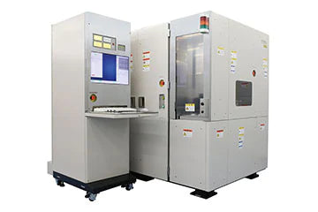
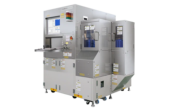
A Defect Review SEM is a Scanning Electron Microscope (SEM) that is configured to review defects found on a wafer. A defect detected by a semiconductor wafer defect inspection system is enlarged using an Review SEM to a high magnification image so that it can be reviewed and classified. A Defect Review SEM is mainly used together with the inspection systems in the production lines of electronic devices and other semiconductors.
The "minimization of design" rule for semiconductor device manufacturing is advancing at a remarkable rate. Recent advancements in techniques make it possible to control device structures at an atomic level. To this end, electron microscopy has become an indispensable technique allowing high-resolution imaging with a quick turnaround time. The electron microscope is able to cover a very wide scale range for evaluating everything from the packaged device to the atomic level gate structure.
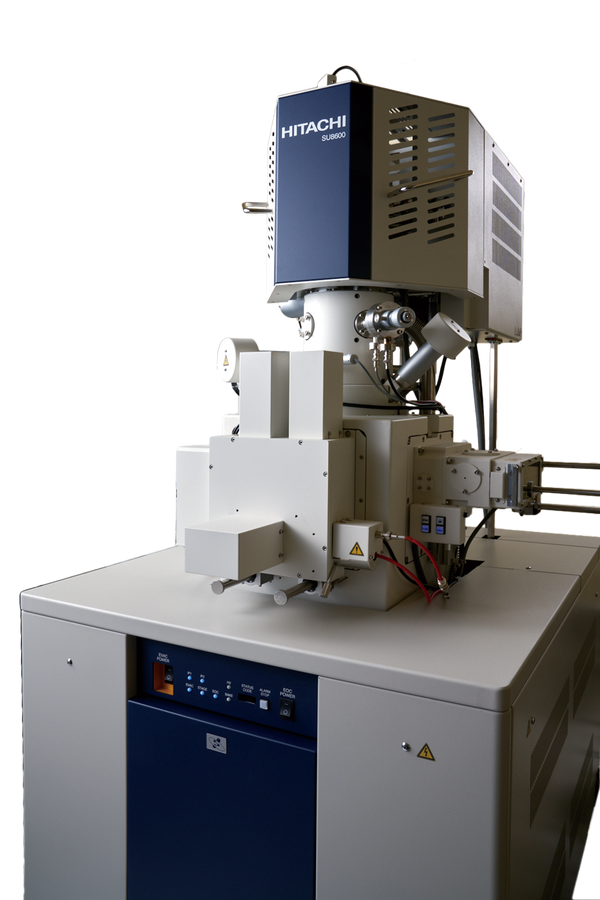
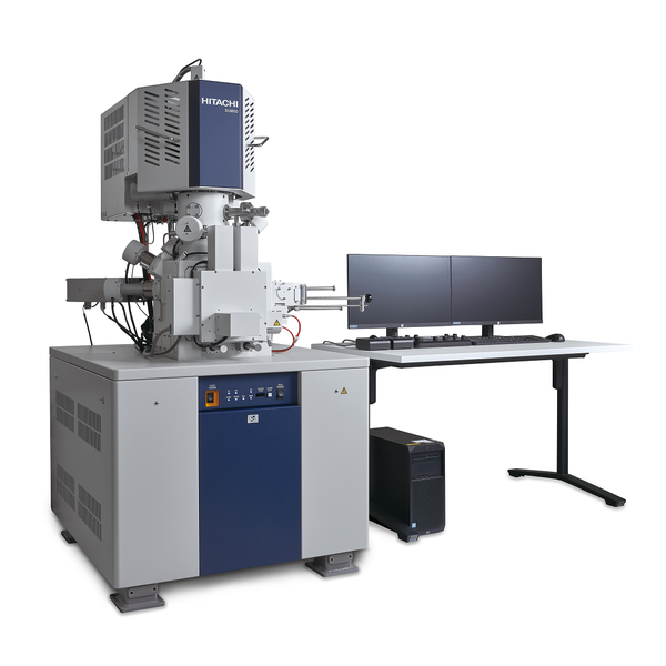
Hitachi High-Tech offers highly advanced in-line and off-line analysis systems for semiconductor device development, manufacturing, failure analysis and quality assurance. We produce a wide range of electron microscope solutions including the world's leading FE-SEM, FIB-SEM, and TEM systems.
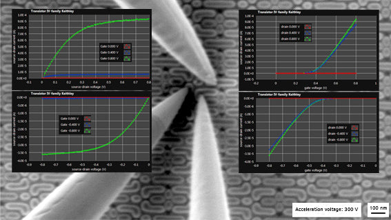
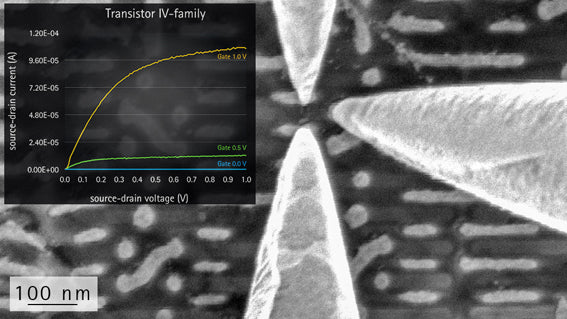
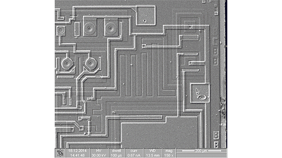
For integrated circuits it is possible to both image and measure properties. Voltage contrast and current imaging can show small variations in electrical properties caused by an added dopant element in minute concentration. It is possible to image conductive paths or broken connects.
Contamination particles can be counted and characterized.
Lithography focus exposure matrices can be evaluated.
Critical dimensions can be measured on both photoresist surfaces and on the developed wafer.
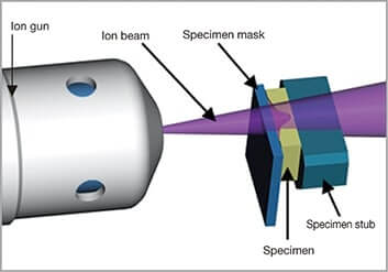
Inspecting printed circuit boards or packaged components often involves cutting into components to understand possible failure reasons inside.
This can involve soldering, bonding issues or delayering problems for example. Also looking at interconnects like Through Silicon Vias (TSV) to understand why circuits are not performing to expectation.
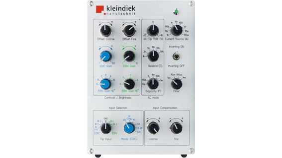
Techniques like EBIC (Electron Beam Induced Current) or EBAC (Electron Beam Absorbed Current) help to understand current flow within a component.