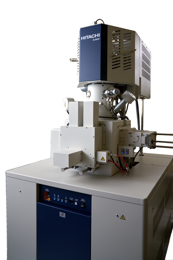

CD-SEM
A Critical Dimension SEM (CD-SEM: Critical Dimension Scanning Electron Microscope) is a dedicated system for measuring the dimensions of the fine patterns formed on a semiconductor wafer. CD-SEM is mainly used in the manufacturing lines of electronic devices of semiconductors.
Three main CD-SEM features that differ from the general-purpose SEM:
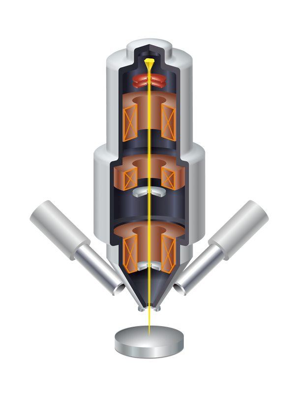
1) CD-SEM primary electron beam irradiating to the sample has low energy of 1keV or below.
Lowering the energy of the electron beam of CD-SEM can reduce the damage to the sample due to charge-up or electron beam irradiation.
2) CD-SEM measurement accuracy and repeatability is guaranteed by improving magnification calibration to the maximum extend.
Measurement repeatability of CD-SEM is around 1% 3σ of the measurement width.
3) Fine pattern measurements on the wafer are automated.
A sample wafer is put inside a wafer cassette (or a Pod / FOUP), which is placed on the CD-SEM. The condition and procedures of the dimensional measurement are input into a recipe* in advance. When the measurement process is started, the CD-SEM will automatically take the sample wafer out of the cassette, load it into the CD-SEM and measure the desired positions on the sample. When the measurement is finished, the wafer will be returned to the cassette.