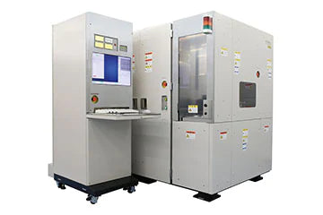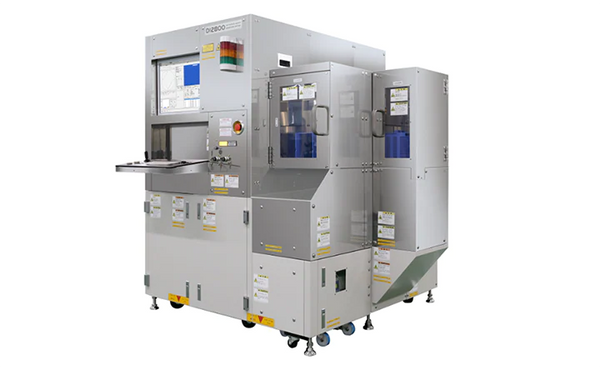

Defect Inspection & Review
Defect detection and review generally works in the following way:
1. Wafer defects are detected using an inspection system which lists position coordinates of the defects and outputs it into a file.
2. The inspected wafer and the file of the inspection result are loaded into the Review SEM.
3. Images of the defects on the list are taken.
The defect position is determined based on the position information from the defect list. Images of the defects are then taken and stored by the Review SEM.
Several thousand to several tens of thousand defects are detected using the inspection system, and the data is output into a file. Whether to review and to take photos of all or some of the defects can be specified in the operation settings of a recipe of the Review SEM.
Sometimes a defect on a wafer cannot be found using the position information in the defect data file. Because of various errors, it is not easy to find a defect using the position information alone.
In a defect inspection system, the defective image is compared with the adjacent die image (reference image) and the defect is detected due to the image difference (difference image processing).
The Review SEM, similar to the defect inspection system, detects the defect by comparison with the circuit pattern of the adjacent die and obtains the correct position of the defect. The defect is then moved to the center of the field of view and an enlarged photo is taken of it.
In the case of Memory IC's defect review, in which cell patterns are arranged repeatedly, the image of the minimum unit of a cell is registered as the reference image in advance. One method of detecting a defect on the Review SEM is to compare the image of the defect with the reference image using difference image processing. This method can speed up the defect detection on the Review SEM because multiple sections can be compared with the same reference image.