You deserve the optimal experience.
Why not add another of these best sellers to your cart?

The SU9000 is HITACHI's new premium SEM. It features unique electron optics, with the sample positioned inside a gap between the upper and lower parts of the objective lens pole piece. This so-called true in-lens concept - combined with the next generation of HITACHI's cold field emission technology - guarantees the highest possible system resolution (SE resolution 0.4 nm @ 30 kV, 1.2 nm @ 1 kV without requiring beam deceleration technology [0.8nm with beam deceleration]) and stability.
The Cold Field Emission source is ideal for high-resolution imaging with a small source size and energy spread. Innovative CFE Gun technology contributes the ultimate FE-SEM with superior beam brightness and stability, affording high-resolution imaging and high-quality elemental analysis. Unique object lens design has a capability of EELS and diffraction as well.

Sample : ArF Resist
Vacc : 500 V
Signal : SE image
No beam deceleration
To make this resolving power usable in practical applications in your lab, the SU9000 utilizes an ultra-stable side-entry sample stage similar to high-end TEM systems and incorporates optimized vibration damping and a closed cabinet to shield the electron optics from environmental noise. Furthermore, the clean vacuum concept of the SU9000 offers a vacuum level in the gun and sample chamber that is one order of magnitude better than the previous generation, thereby minimizing sample contamination artifacts (effective pre-observation cleaning of the samples themselves can be achieved using Hitachi's ZONESEM sample cleaner).
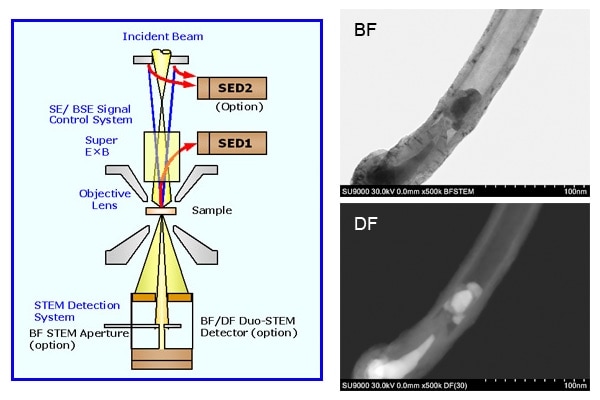
In addition to pure, unsurpassed resolution, the SU9000 is also equipped with a remarkable 2+2 detection system for sample surface, composition and transmission observations.
The combined use of the patented Super ExB filter with the first upper detector allows users to filter and collect SE and LA-BSE signal energies of interest, thereby suppressing charging artifacts and showing topographical details, and the top detector selectively receives HA-BSE signals, providing topography-free information of material and crystallographical orientation differences. This signal selection technology makes the SU9000 a preferred system for catalyst and other areas of research as well as for biological and pharmaceutical immunolabeling applications when used in combination with a cryogenic sample holder.
The SU9000 is also an incredibly powerful low-kV STEM, often exhibiting higher contrast on critical sample features than high-energy S-TEM systems. In addition, simultaneous Brightfield and annular Darkfield imaging is possible with the Darkfield detector settable to 56 different positions for an optimized selection of Z-contrast of the pattern of interest.
The stunning stability of the SU9000 allows a guaranteed STEM resolution specification of 0.34 nm, enabling the observation of graphite lattice fringes for example in a carbon nanotube.
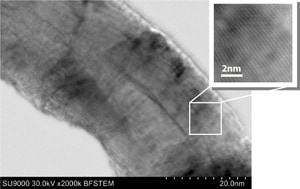
Sample : Multi wall carbon nano tube (lattice fringes)
Vacc : 30 kV
Mag. : 2,000kx
Bright Field(BF)-STEM image
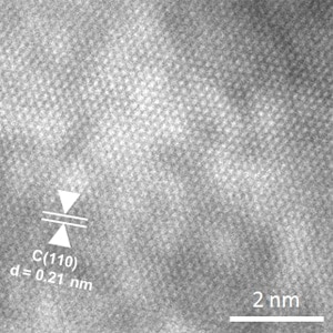
Sample : Graphene (lattice fringes)
Vacc : 30 kV
Mag. : 3,000kx
Bright Field(BF)-STEM image
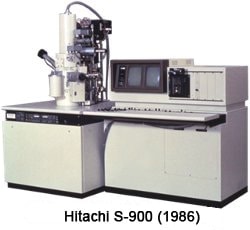
S-900 launched with 1,000 units installed.
In 1986, Hitachi released the S-900, the world's first commercial in-lens FE-SEM. With 0.8 nm SE resolution and a usable magnification of up to 800.000x, the new concept of the S-900 truly opened up a new world for researchers in many fields.
The success story continued with the S-5000 (1990), S-5200 (2000) and S-5500 (2004), with each new model setting new standards.
In 2011 Hitachi celebrated 25 years of in-lens FE-SEM technology, and used that opportunity to introduce the new SU9000, the most powerful member in Hitachi's high-end FE-SEM product line-up.
Investigating samples with the full capabilities of STEM at 30 keV and below is an extremely interesting and rapidly growing area of research: providing both Materials and Life Sciences with full SEM and STEM, inclusive EDX, and EELS capabilities, at low voltages. Less beam damage and higher contrast are the key arguments for the Low-Voltage STEM (LV-STEM), a capability that has been out of reach for researchers globally. With the LV-STEM, its low beam energy, increased contrast, and narrow energy spread, investigations of biological material in an unstained condition are becoming a reality for the first time.
Since the STEM unit has no imaging lens after the sample, electrons that were inelastically scattered by the sample do not really worsen image quality (they do for TEM). The significance of the lack of chromatic aberrations after the sample increases with decreasing electron energy; samples that typically would require a 100-keV TEM, at the very least, can be investigated with low-keV STEM. Multi-scattering processes and absorption of course still appear—ultimately limiting the acceptable thickness of the specimen. However, the use of high-end specimen preparation techniques, or working with thin samples as is typical in nano-research fields, allows 30-keV STEMs to cover much of the areas of conventional higher-keV TEMs, while at the same time, providing surface information through standard SEM methods, including SE, BSE, and high-angle BSE.
The well-established cold FEG of Hitachi’s high-end SEMs is a tremendous benefit for EELS capabilities as well as the point resolution of STEM. Despite the unusually low voltage for EELS and the increased impact of environmental conditions on low-voltage electrons, we are able to demonstrate better than 400-meV FWHM (full width half maximum, see Figure 1, left) for the ZLP (zero loss peak) of EELS, allowing clear and crisp EELS data for fine structure investigations. For example, eliciting the tiny changes in the π bonding for the Graphene as layer after layer is added demonstrates the sensitivity of the LV-STEM (see Figure 1, right). The LV-STEM also has a 2nd dedicated EELS detector with 3 elements, allowing the rapid (10,000 fps) acquisition of energy-filtered BF STEM images, Plasmon images, or the rapid collection of elemental maps. Switching between both detectors is easy and relies on Hitachi’s own unique design.
The LV-STEM feature (Figure 2) complements SE imaging and makes no compromise. Typical images taken at 30 keV without a Cs corrector or Cc corrector approach 0.2-nm resolution establishing the LV-STEM as the true performance leader for ≤ 30 keV microscopy. The importance of simultaneously acquiring STEM and SE data is demonstrated in Figure 3.
As this microscope can handle samples up to 5.0 mm × 9.5 mm × 3.5 mm, the optional windowless EDX detector supports the analysis of both thin and bulk areas. At an incredible collection angle of 0.7 sr, acquisition times for EDX maps are short (see details in Figure 4), making the LV-STEM a truly ground-breaking microscope for both Materials and Life Sciences applications.
References
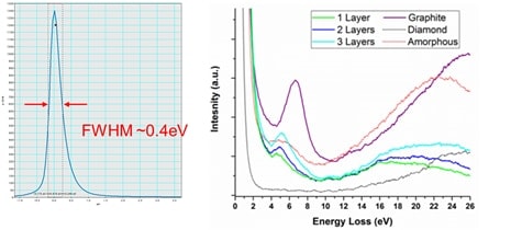
Figure 1 Left: despite the low (± 30 keV) energy of these electrons, the energy spread of the electron beam, measured by our own Hitachi EELS is 400 meV or less:. Right: EELS spectra differentiating between single , double and triple layers of graphene , graphite, diamond, and amorphous carbon.
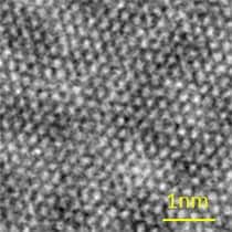
Figure 2 The low-pass-filtered BF STEM of Graphene at 30 keV shows a resolution of close to 0.2 nm; the 0.142 nm atom distances are not resolved.
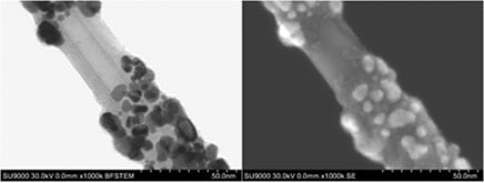
Figure 3 Left: The high-resolution 30-keV BF STEM image by itself makes it difficult to model its 3D structure. Right: Only in combination with the (simultaneously acquired) high-resolution SE image, the real structure of this sample becomes obvious and modeling this structure as a 3D model would be quite manageable.
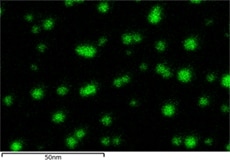
Figure 4 Elemental EDX map (Au M) at 30 kV, The size of the nano-particles is in the range of 5-10 nm. Acquisition time is 3.5 min at a current of 1 nA
